


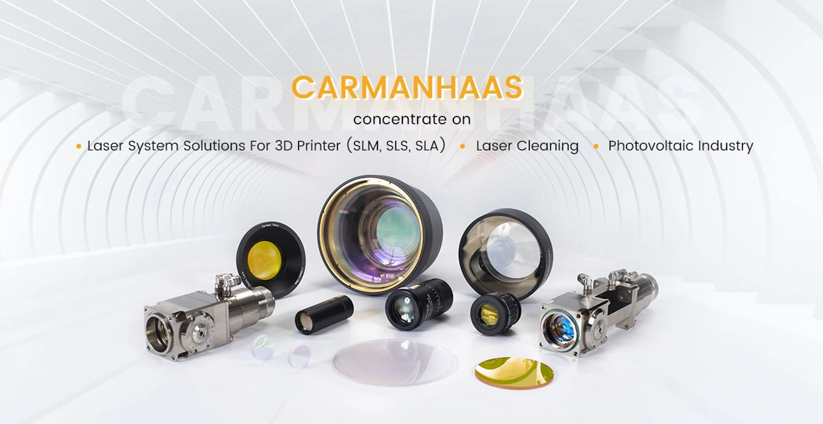


Laser cutting technology VS solar cell
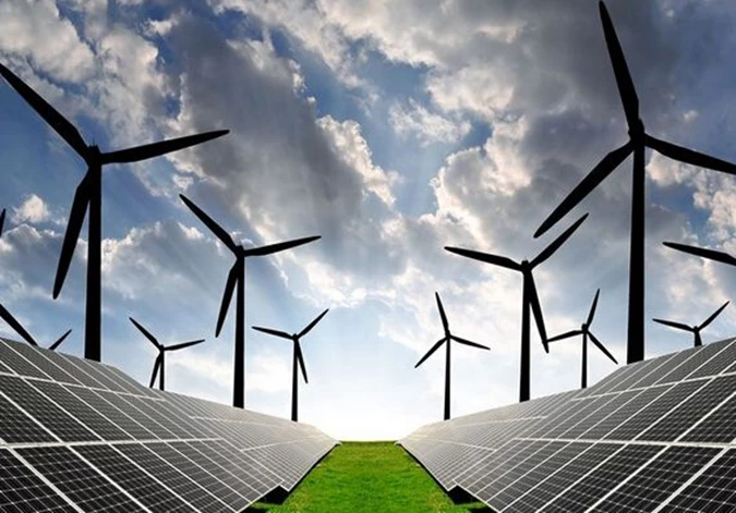
As the global shortage of primary energy becomes more and more severe, the development and utilization of clean energy has become an urgent problem for all industries around the world. Solar cell is a device that can convert light energy into electrical energy, mainly silicon-based solar cells, which can effectively reduce environmental pollution and energy consumption crisis.
As one of the clean, pollution-free and renewable energy sources, solar cells have promoted the rapid development of the photovoltaic industry and played a very important role in the development of the photovoltaic industry.
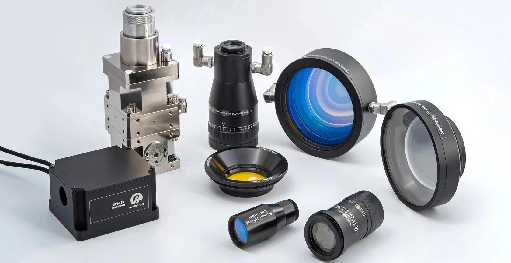
optical system for laser processing onsolar cell
Solar cells are divided into compound solar cells, silicon solar cells, organic thin-film solar cells, and dye-sensitized solar cells according to different materials. Among them, silicon solar cells are widely used, so they are divided into polycrystalline silicon solar cells. Cells, monocrystalline silicon solar cells and amorphous silicon solar cells. In the manufacturing process of crystalline silicon solar cells, laser cutting technology is mainly used for cutting wafer cutting and dicing cutting.
Laser cutting technology plays a very important role in the field of solar cells. Compared with other processing technologies, laser cutting technology is more efficient. On the one hand, it improves process reliability and on the other hand reduces production costs. These advantages have been fully embodied in the production of crystalline silicon solar cells and thin-film solar cells.
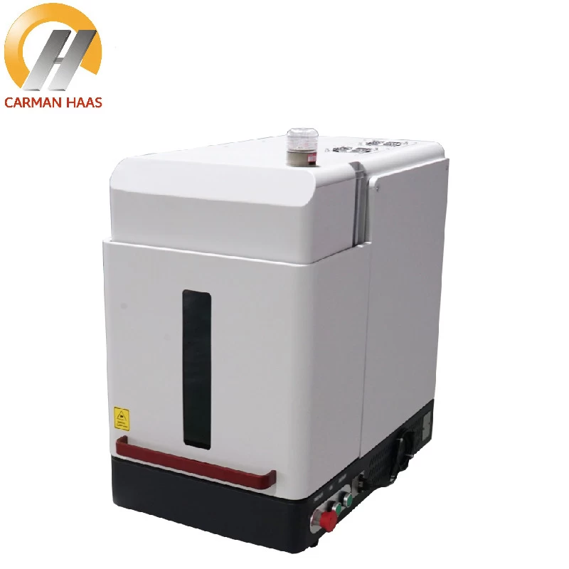
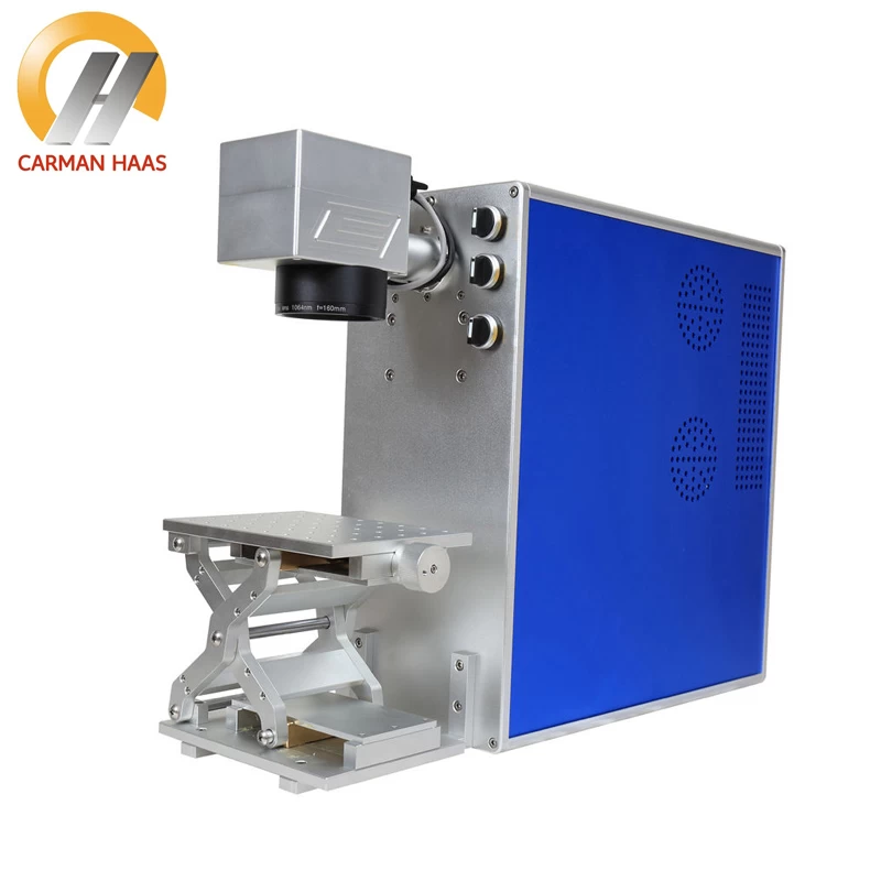
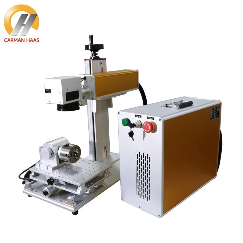
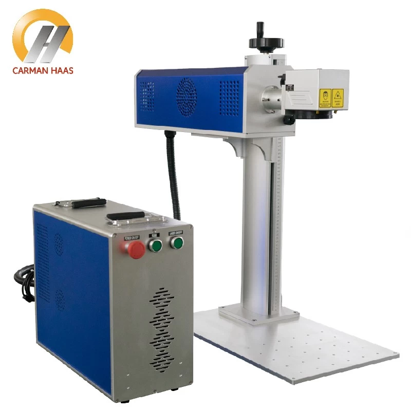
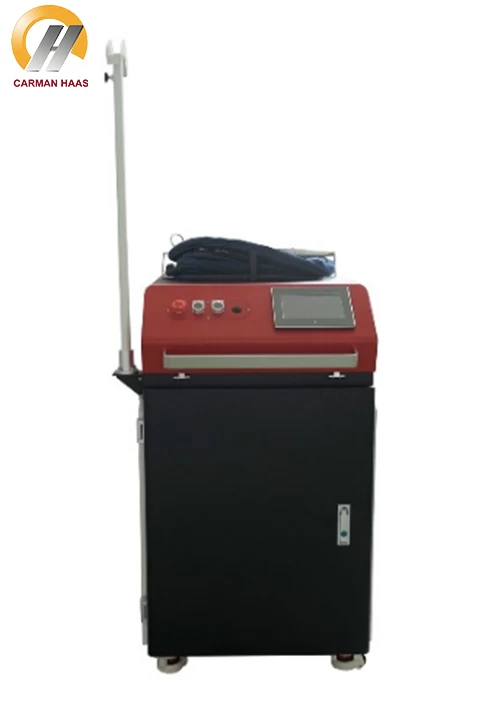
Laser cutting machine wholesale
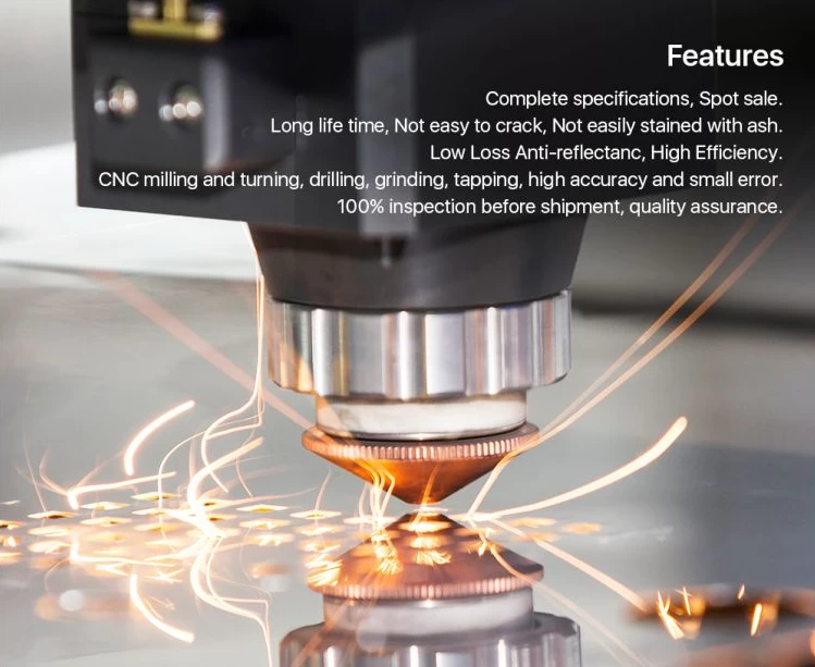
Compared with traditional methods, laser cutting technology has unique advantages, mainly as follows
1) The cutting precision is high, the cutting seam is narrow, the quality is good, the heat affected zone is small, and the cutting end surface is flat and smooth;
2) Fast cutting speed and high processing efficiency;
3) It is a non-contact processing, without mechanical processing force, no deformation, no pollution problems such as processing chips, oil pollution, noise, etc., and it is a kind of green environmental protection processing;
4) Strong cutting ability, almost any material can be cut.
Cutting and dicing:
Using a laser to scribing and cutting silicon wafers is currently a relatively advanced technical method. Its principle is to use a laser as a cutting scribing tool and also to use the principle of material gasification. The material to be processed is irradiated with a focused laser beam, and then the workpiece is moved. Since the material is removed due to vaporization, the workpiece is cut and diced by the laser along the moving direction.
Features of laser cutting scribing:
1) The laser can be focused into a small spot and can draw very thin lines.
2) The cutting depth is 2 to 3 times larger and can be controlled, which greatly improves the qualified rate of cutting.
3) Non-contact processing, short action time and range of silicon wafer, small heat-affected zone, and no cracks due to mechanical stress.
4) The scribing speed is fast, which greatly improves the productivity, is suitable for automatic control on-line, and reduces the production cost.
5) Scribing can be performed on semiconductor boards coated with a protective layer.
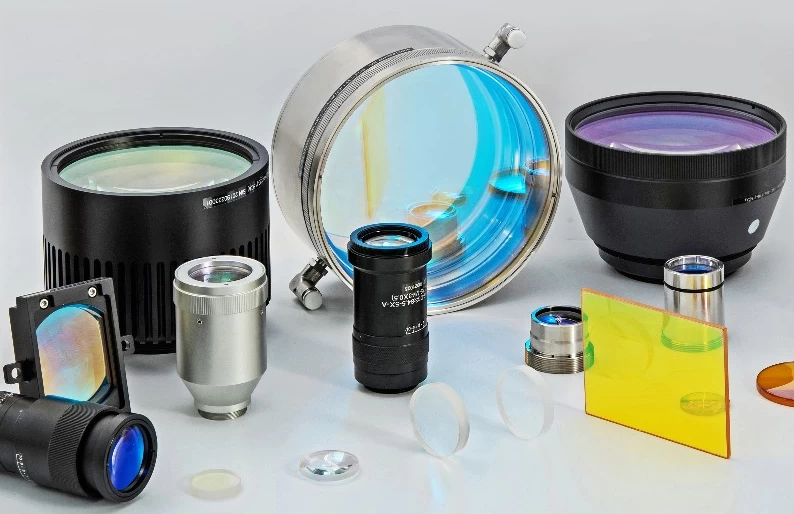
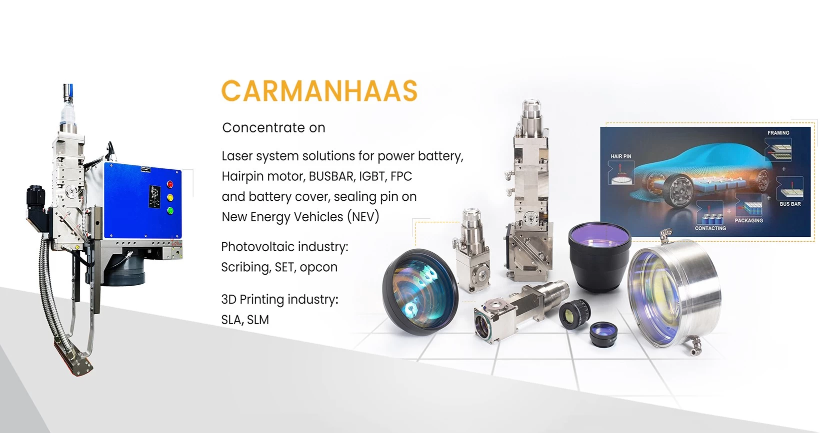
Power battery laser cutting lens
Wafer cutting
Wafer cutting is a more critical process in the production of monocrystalline silicon cells. The monocrystalline silicon materials used in industrially produced silicon cells are generally monocrystalline silicon rods. The original shape is cylindrical and needs to be cut into square silicon wafers, which are usually sliced by wire cutting.
What are the disadvantages of traditional wire cutting compared with laser cutting?
Generally speaking, wire cutting is used, the thickness of the silicon wafer is large, and the cutting flatness is poor. Moreover, since silicon is a brittle material, contact processing is very easy to cause edge cracks. In addition, there will be a mechanical damage layer composed of elastic strain regions, dislocation network regions, and fragmented crystal regions on the silicon surface. The yield is low, the loss of raw materials is large, and it may even cause hidden cracks, affecting electrical parameters and other hazards.