


Application of laser in PCB and FPC manufacturing
With the development of flexible circuits now, smaller and more complex flexible circuit boards will become the future development direction in the future. Traditional processing methods are difficult to meet the processing needs due to their own conditions. In order to achieve more refined flexible circuits Design requires more refined processing solutions. At the same time, the application of lasers on PCBs and flexible circuit boards is becoming more and more extensive!
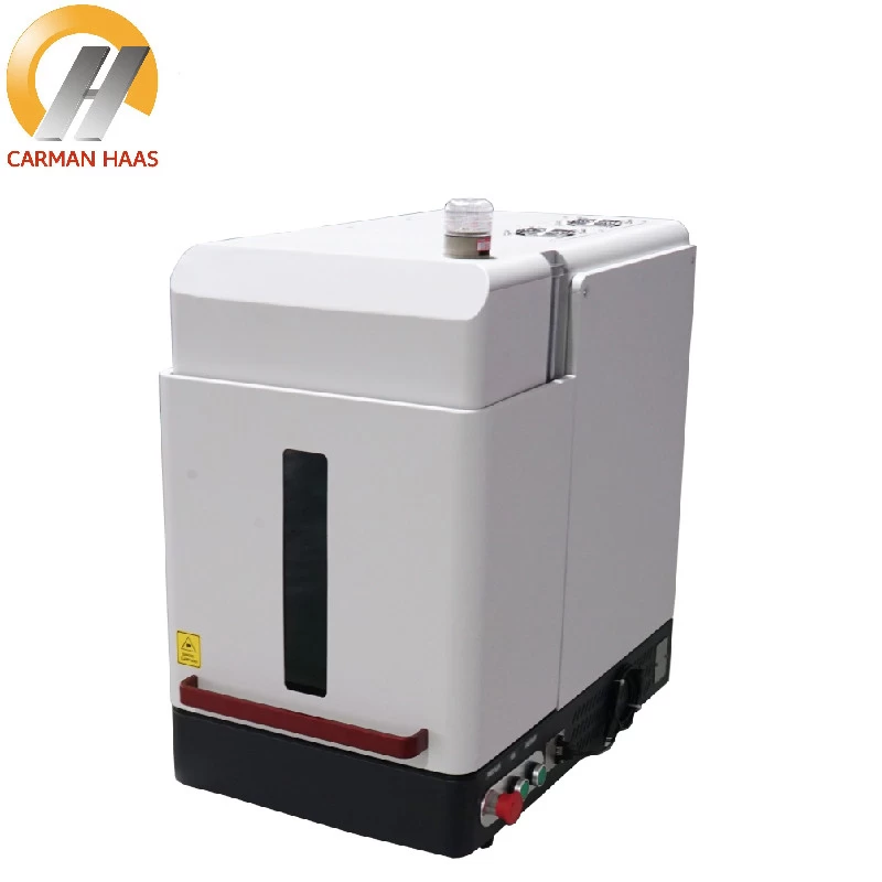
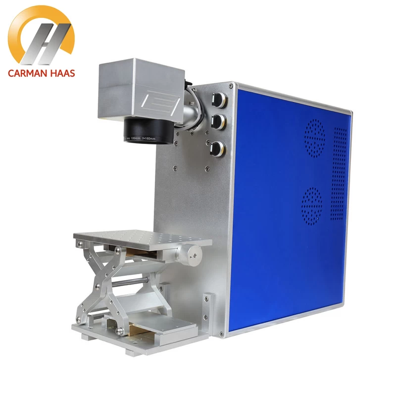
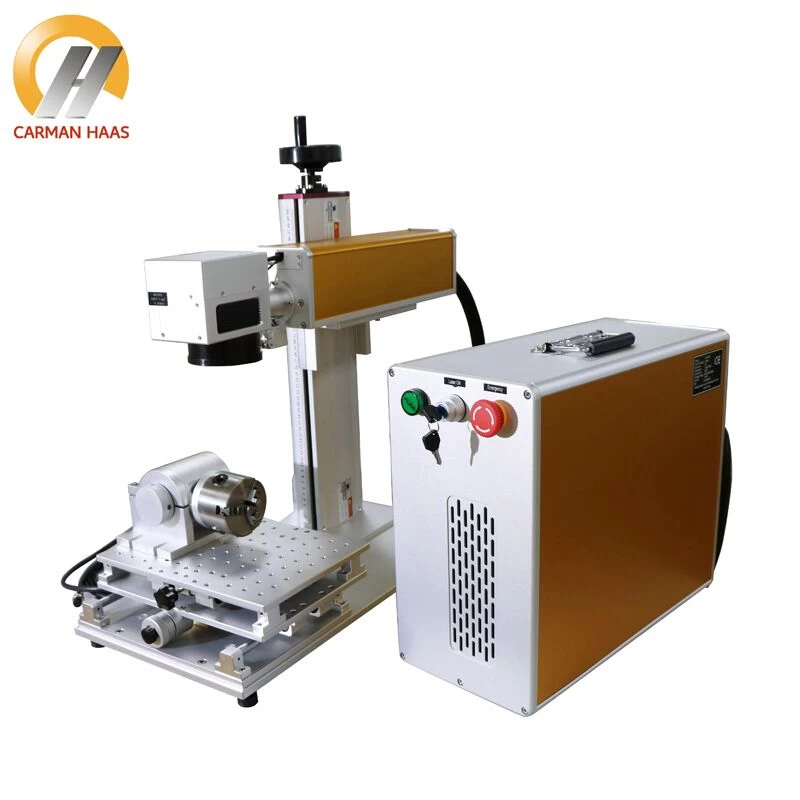
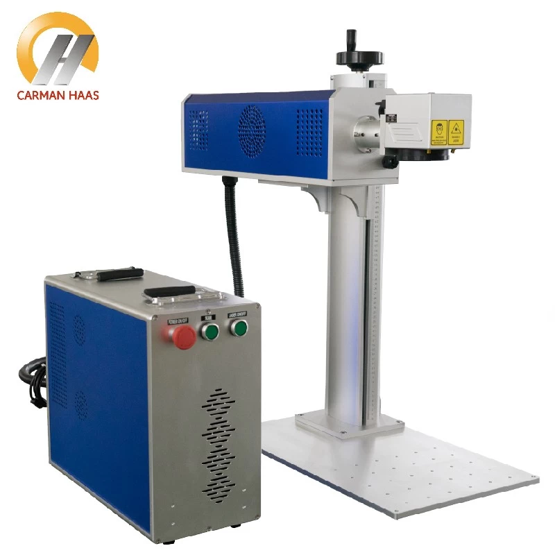
Laser Marking
Laser marking has high precision, fast speed and stable performance. Only need to be controlled by computer, simple operation, can print a variety of complex patterns, text, QR code and other content, non-contact processing, no consumables, environmental protection and no pollution, fully in line with the existing PCB and flexible circuit board industry high-quality marks Claim. Can make up for the shortcomings of silk screen processing, and gradually become the best processing tool for PCB marking, playing a pivotal role in the circuit board industry!
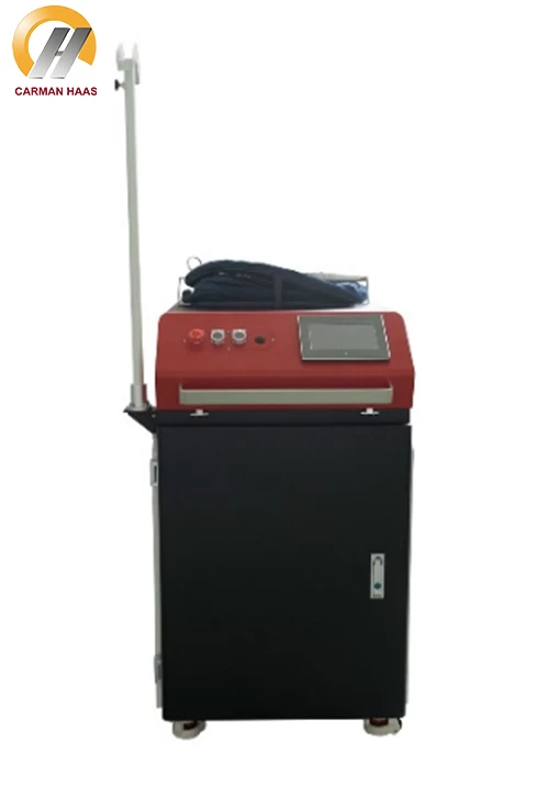
Ultraviolet laser marking machine(UV F-theta lens manufacturer china), with high-energy laser beam, can convert light energy into chemical energy when acting on polymer materials such as PI, and under the action of precision laser beam, it partially connects the chemical bonds of substance atoms and molecules Changes occur to achieve the purpose of surface treatment. During the processing, due to the processing time and energy concentration, the surface of the processed article is almost not damaged. Therefore, whether it is in the processing accuracy or quality, can be effectively guaranteed. Although the current UV laser marking machine is more expensive than traditional processing equipment, the process requirements for marking are difficult to achieve with other processing methods. In the future, laser technology will effectively provide more sophisticated processing solutions for flexible processing, and provide a powerful guarantee for smaller and more complex flexible circuits in the future.
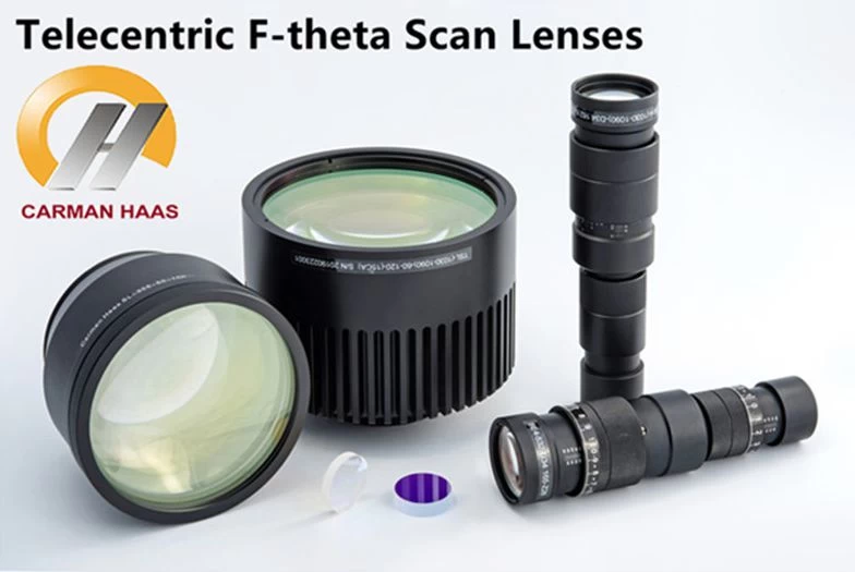
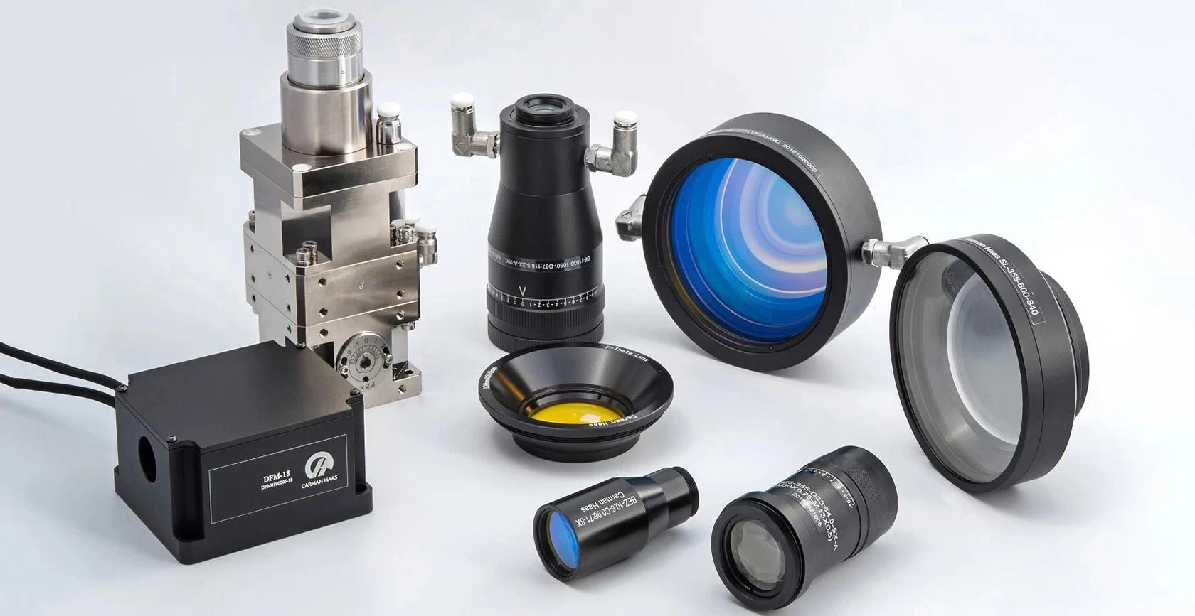
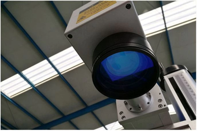
Telecentric lens factory china
Compared with traditional printing technology, laser marking technology has many advantages:
1) Good quality and strong wear resistance. The surface of the PCB board is marked and beautiful, and various LOGO, patterns, QR codes, texts can be marked and the patterns are directly carved on the material, and the wear resistance is more prominent;
2) High processing accuracy. After the laser beam emitted by the laser is focused, the minimum spot diameter can reach 10um (UV laser), which is of great help when processing complex graphics and precision processing;
3) High efficiency, simple operation and reduced cost. Users only need to set the parameters on the computer to directly mark, and the surface marking of the material can be completed in just a few seconds to more than ten seconds;
4) Non-destructive marking. Laser marking uses non-contact processing, the laser head does not need to contact the surface of the material, so there is no need to consider the damage to the material;
5) Wide range of use, safety and environmental protection. All kinds of thin metal/non-metal materials can be marked;
6) Stable performance and long service life of equipment. With the development of technology, the service life of lasers has greatly increased, and the service life of equipment has been greatly