


The mainstream application of laser cutting on solar cells
Cutting and dicing:
Using a laser to scribing and cutting silicon wafers is currently a relatively advanced technology method. Its principle is to use a laser as a cutting scribing tool and also to use the principle of material gasification. The material to be processed is irradiated with a focused laser beam, and then the workpiece is moved. Since the material is removed due to vaporization, the workpiece is cut and diced by the laser along the moving direction.
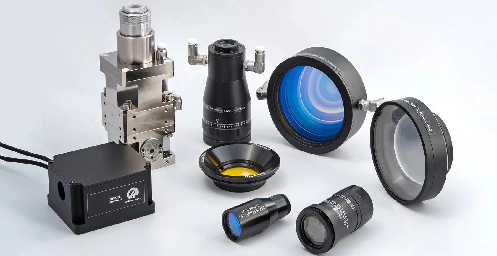
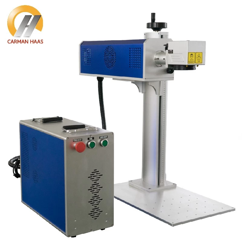
Optical system laser processing onsolar cell
Features of laser cutting scribing:
1) The laser can be focused into a small spot and can draw very thin lines.
2) The cutting depth is 2 to 3 times larger and can be controlled, which greatly improves the qualified rate of cutting.
3) Non-contact processing, short action time and range of silicon wafer, small heat-affected zone, and no cracks due to mechanical stress.
4) The dicing speed is fast, which greatly improves the productivity, is suitable for automatic control on-line, and reduces the production cost.
5) Scribing can be performed on semiconductor boards coated with a protective layer.
Wafer cutting
Wafer cutting is a more critical process in the production of monocrystalline silicon cells. The monocrystalline silicon materials used in industrially produced silicon cells are generally monocrystalline silicon rods. The original shape is cylindrical and needs to be cut into square silicon wafers, usually by wire cutting.
What are the disadvantages of traditional wire cutting compared with laser cutting?
Generally speaking, wire cutting is used, the thickness of the silicon wafer is large, and the cutting flatness is poor. Moreover, since silicon is a brittle material, contact processing is very easy to cause edge cracks. In addition, there will be a mechanical damage layer composed of elastic strain regions, dislocation network regions, and fragmented crystal regions on the silicon surface. The yield is low, the loss of raw materials is large, and it may even cause hidden cracks, affecting electrical parameters and other hazards.
Using laser precision cutting technology instead of wire cutting, due to its non-contact processing, no stress, so the cutting edge is flat and steam, no damage, no damage to the wafer structure, electrical parameters are better than mechanical cutting methods, which improves the yield. Reduced costs. At the same time, the characteristics of small slit width, high precision, and adjustable laser power also enable the application of laser precision cutting technology to control the cutting thickness, thereby making it possible to achieve thinning of solar cells.